ADC and DAC, PCF8591 (YL-40)
Four 8-bit inputs and one analog output on I2C at 0x48, with the YL-40 board LDR, thermistor and trimmer on jumpers.
- 9 pins
- 1 setting
- In 1 project
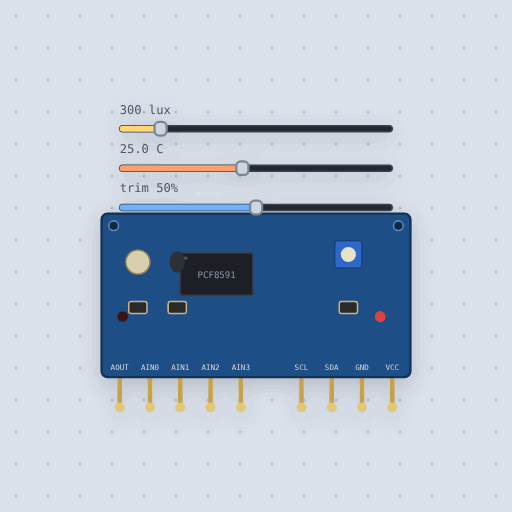
The ADC and DAC, PCF8591 (YL-40) in brief
What it is, and every setting the properties panel gives it.
The PCF8591 on the YL-40 module gives four 8-bit analog inputs and one analog output over I2C, which is why it is the analog board in the Freenove and SunFounder kits and the way a Raspberry Pi, which has no analog inputs, reads a sensor. On the board three inputs carry sensors on jumpers: a light-dependent resistor on AIN0, a thermistor on AIN1 and a blue trimmer on AIN3. Each is a divider, with the LDR and thermistor under 10 kilohm pull-ups, so more light and more heat both read lower. Mokxi follows the NXP datasheet. Each read starts a conversion and sends the result of the one before, so the first byte after power-on is 0x80. It models all four input modes, auto-increment, and the DAC, which puts the supply times the value over 256 on AOUT while enabled. The converter’s offset and gain errors and the oscillator are not modeled.
- Family
- Sensors
- Pins
- 9
- jumpers
- true
- on (as shipped) puts the board's own sensors on three inputs, the
light-dependent resistor on
AIN0, the thermistor onAIN1and the blue trimmer onAIN3. Off, every input is yours.
9 pins
Named as the editor names them, so a wire lands where you expect it.
How to use the PCF8591 (YL-40) analog board with an Arduino
Four wires do it: VCC to 5 V, GND to ground, SDA to A4 and SCL to A5. The module answers at 0x48. With its jumpers fitted, the three sliders on the part are the light on the LDR, the temperature at the thermistor and the trimmer’s position, and the LED beside AOUT lights with the DAC’s voltage. The built-in project reads light on channel 0, temperature on 1 and the trimmer on 3, then copies the trimmer to the DAC so turning it brightens the LED.
The surprise is in the readings. The chip sends the conversion before the one just asked for, which is why every tutorial reads twice, and the Adafruit library hides it. The LDR reads lower in more light and the thermistor lower when warmer, because each sits under a 10 k pull-up. The DAC puts VCC times value over 256 on AOUT, so 200 gives about 3.9 V on 5 V.
Take the jumpers off before wiring a sensor of your own to AIN0, AIN1 or AIN3, or the board’s sensor fights it as it would on the real board. With the jumpers off every input is yours. The converter has four single-ended inputs, three differential against AIN3, a mixed mode and two differential pairs, and differential results are two’s complement from minus 128 to 127.
The chip runs from 2.5 V to 6 V and the input range is 0 V to its supply. A 3.3 V board gives a 3.3 V range, and the same two wires let a Pico or a Raspberry Pi read analog sensors.
#include <Wire.h>
#include <Adafruit_PCF8591.h>

Adafruit_PCF8591 pcf = Adafruit_PCF8591();

void setup() {
  Serial.begin(9600);
  pcf.begin();             // 0x48
  pcf.enableDAC(true);
}

void loop() {
  uint8_t trim = pcf.analogRead(3);   // 0 to 255
  pcf.analogWrite(trim);              // AOUT follows the trimmer
  Serial.println(trim);
  delay(250);
}
Common ADC and DAC, PCF8591 (YL-40) errors and fixes
Questions and answers
What does the PCF8591 do?
It reads four analog inputs with an 8-bit converter and drives one analog output with an 8-bit DAC, all over I2C at address 0x48.
Why does it need two reads?
Each read starts a conversion and sends the result of the one before. The first byte after power-on is 0x80. A sketch that switches channel and reads once gets the old channel.
How do I use the DAC?
Enable it, then write a value from 0 to 255. AOUT becomes VCC times value over 256, about 3.9 V for 200 on 5 V, with an assumed 50 ohm source resistance in the model.
Which library reads the PCF8591?
Adafruit_PCF8591. Mokxi compiles it, and the project uses analogRead(), analogWrite() and enableDAC().
What is true about the ADC and DAC, PCF8591 (YL-40), here
In its help article’s own words: what the simulation gets right, and where it stops.
Modeled
From the NXP datasheet:
The read is one conversion behind. Each read starts a conversion and sends the result of the one before; the first byte after power-on is 0x80. A sketch that switches channel and reads one byte gets the old channel's value, which is why every tutorial reads twice.
All four input modes. Four single-ended inputs; three differential (each
against AIN3); two single-ended and one differential; or two differential.
Differential results are two's complement, -128 to 127.
Auto-increment walks the channels after each conversion, wrapping at the mode's channel count.
The DAC puts VCC x value / 256 on AOUT while it is enabled and leaves the
pin high impedance when it is not.
The board's dividers. The LDR and the thermistor each sit under a 10 k pull-up, so more light and more heat both read lower; the trimmer is across the supply. Each drives its input as the divider it is, so a wire you add to the same input fights it as it would on the real board.
Not modeled
The converter's offset and gain errors (a few counts on a real chip), the
oscillator and its output, the external reference (the YL-40 ties it to the
supply, as here), and the load of the LED on AOUT. The DAC buffer's source
resistance is an assumed 50 ohm.
From PCF8591 ADC and DAC (YL-40), in full.
See the ADC and DAC, PCF8591 (YL-40) in a project
One built-in project uses it. It opens in the editor, already wired.
The boards it is shown on
This board has a built-in project with the ADC and DAC, PCF8591 (YL-40) in it.
The rest of the bench
Every one of these is drawn and simulated the same way.
Wire up the ADC and DAC, PCF8591 (YL-40)
Open the editor and push it into the breadboard. It is free, and it runs on your own machine.