74HC4051 analog multiplexer
Eight channels to one pin through analog switches: three address lines pick which one.
- 16 pins
- 1 setting
- In 1 project
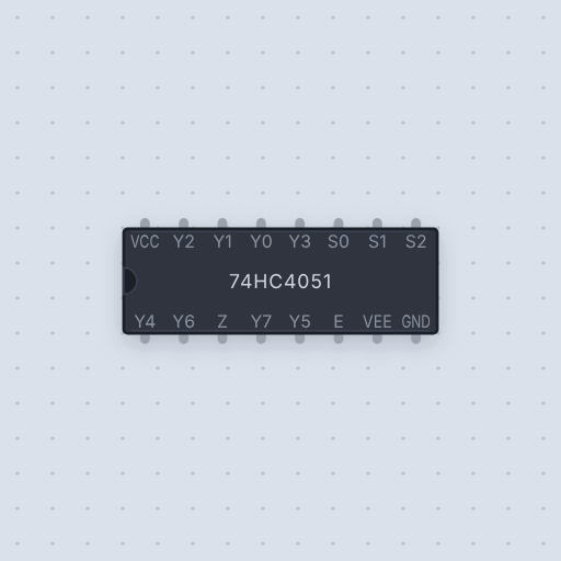
The 74HC4051 analog multiplexer in brief
What it is, and every setting the properties panel gives it.
The 74HC4051 is an 8 channel analog multiplexer, eight analog switches with one common pin in a 16 pin DIP: three address lines pick which channel reaches Z. The pins are Y0 to Y7, the eight channels, Z, the common pin, S0, S1 and S2, the channel address with S0 the least significant bit, E, enable, active low, which opens every switch when high, VEE, the negative analog supply, tied to GND on an Arduino, and VCC and GND, 2 to 6 V. Each switch passes current in either direction, so one analog pin reads eight sensors, or one pin drives eight outputs in turn. The model property picks the 74HC4051 or the CD4051B, which runs from 3 V to 18 V with a much higher on-resistance: 470 ohms against 70.
- Family
- Logic
- Pins
- 16
- model
- 74HC4051 (or CD4051B)
16 pins
Named as the editor names them, so a wire lands where you expect it.
GND.S0 the least significant bit.S0 the least significant bit.S0 the least significant bit.How to read eight knobs on one analog pin with a 74HC4051
Z, the common pin, goes to A0. The three address pins S0, S1 and S2 go to Uno pins 2, 3 and 4. E, enable, VEE and GND all go to ground: E low turns the switches on, and VEE is tied to GND on an Arduino. VCC is on 5 V. The three knobs’ wipers go to Y0, Y1 and Y2.
The sketch writes the channel number onto the three address pins, bit 0 to S0, waits 50 microseconds for the switch to settle and reads A0. It reads channels 0, 1 and 2 and prints them every 300 ms. The same pins would read eight channels. The 74HC4051 is the smaller cousin of the CD74HC4067, which has sixteen.
const uint8_t ADDRESS[3] = {2, 3, 4};   // S0, S1, S2

int readChannel(uint8_t channel) {
  for (uint8_t bit = 0; bit < 3; bit++) {
    digitalWrite(ADDRESS[bit], (channel >> bit) & 1 ? HIGH : LOW);
  }
  delayMicroseconds(50);                 // let the switch settle
  return analogRead(A0);                 // Z is on A0
}

void setup() {
  Serial.begin(9600);
  for (uint8_t bit = 0; bit < 3; bit++) pinMode(ADDRESS[bit], OUTPUT);
}

void loop() {
  for (uint8_t ch = 0; ch < 3; ch++) {
    Serial.print("Y");
    Serial.print(ch);
    Serial.print(" ");
    Serial.print(readChannel(ch));
    Serial.print(ch < 2 ? "  " : "\n");
  }
  delay(300);
}
Common 74HC4051 analog multiplexer errors and fixes
Questions and answers
How many analog pins does a 74HC4051 save?
It reads eight sensors on one analog pin and three digital pins.
What is the difference between the 74HC4051 and the CD4051B?
Same pins. The CD4051B runs 3 V to 18 V and has a much higher on-resistance: 470 ohms typical at 5 V against 70 ohms.
Can the 74HC4051 output as well as input?
Yes. Each switch passes current in either direction, so one pin can drive eight outputs in turn.
What is true about the 74HC4051 analog multiplexer, here
In its help article’s own words: what the simulation gets right, and where it stops.
Modeled
From the Nexperia 74HC4051 and TI CD74HC4051 datasheets: E low joins the
addressed channel to Z through the switch's on-resistance, both ways round, and
leaves the others open; E high opens them all. The on-resistance is about 70
ohm at 4.5 V and more at lower supplies, so a load on Z divides against it.
The address and enable are CMOS inputs read against half the supply; an address
that is not a clean level opens every switch.
Not modeled
The switching time, break-before-make, charge injection, leakage, the
on-resistance's change with the signal voltage, and signals below ground: VEE
is not read, as if it were tied to GND.
From 74HC4051 8-channel multiplexer, in full.
See the 74HC4051 analog multiplexer in a project
One built-in project uses it. It opens in the editor, already wired.
The boards it is shown on
This board has a built-in project with the 74HC4051 analog multiplexer in it.
The rest of the bench
Every one of these is drawn and simulated the same way.
Wire up the 74HC4051 analog multiplexer
Open the editor and push it into the breadboard. It is free, and it runs on your own machine.